
INTRODUCTION
| The packaging laboratory comprises all the equipment necessary to separate a substrate wafer in dies and electrically and fluidically connect the die into a package. |
| HIGH PRECISION DICING SAW | |
|
|
MODEL ADT7100
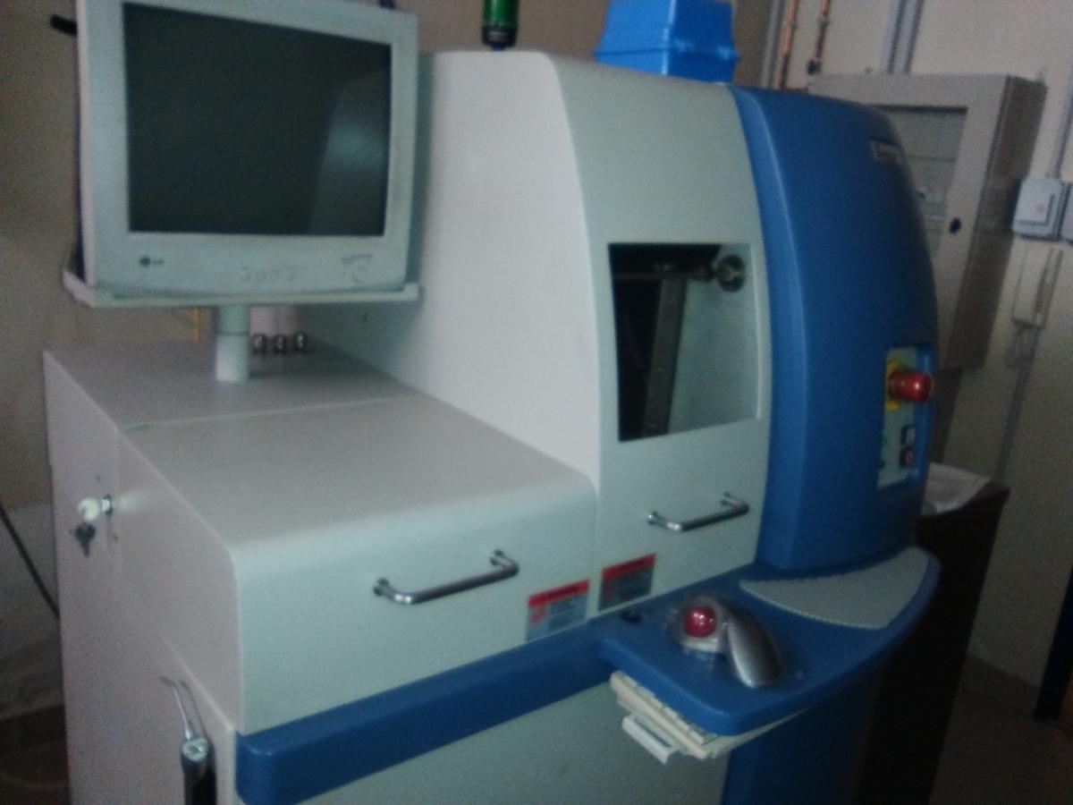
The ADT 7100 Dicing Saw is optimized for multi-angle dicing of thin, tight tolerance products up to 150 mm or 6" diameter. It is capable of more complex patterns such as multiple indexes and varying cut depths with an accuracy of about 2 µm. Cut Depth and width depends on the blade and flange diameter: about 1,2 mm depth and 40-200 µm width. The material that can be cut are: Silicon, Fuse Silica, Pirex, LiNbO3, SiC up to 1mm thick. |
| MANUAL WADGE WIRE BONDING | |
|
|
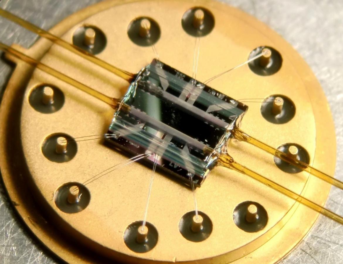
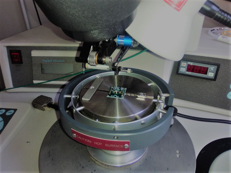
Kulicke & Soffa 4523 AD Manual wedge wire bonding equipment. It provides electrical interconnections between chip pads and package pads by means of wire bonding activated by ultrasound. Manual X-Y sample positioning. Main parameter managed during wire bonding process are Power, Force Time applied to each bonding. Capability to manage Al-Si or Gold wires. Usual wire diameters are 25µm and 18µm. Option for Deep Access tools is available. |
| WAFER BONDING & BONDER ALIGNER | |
|
|
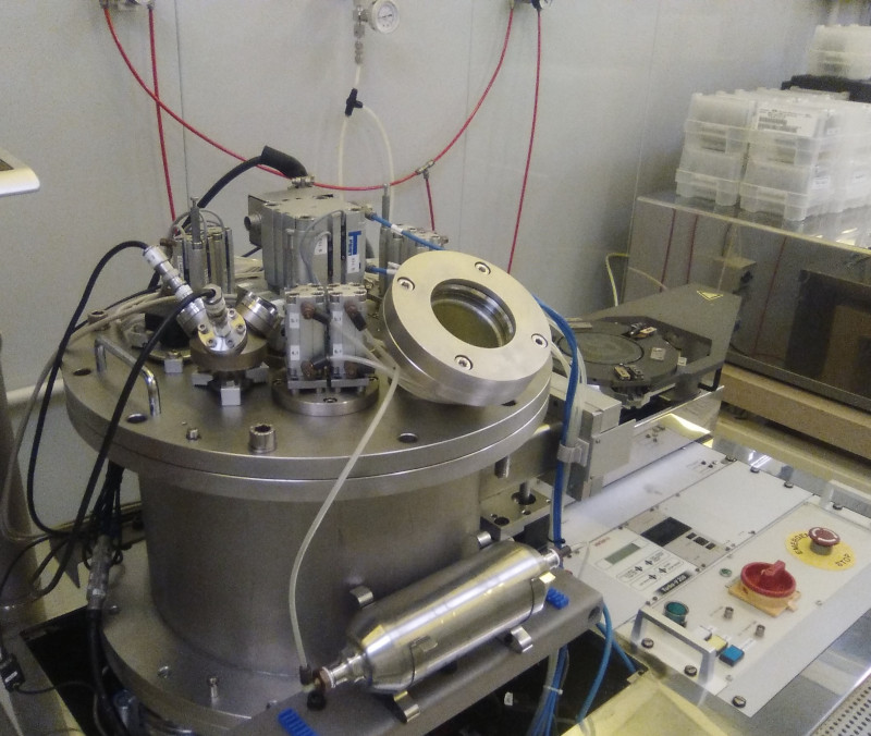
WAFER BONDER SB6 SuSS Microtec
WAFER ALIGNER BA6 SuSS Microtec
|
| MICRO/NANO FABRICATION HOME PAGE |