
The characterization of materials plays an important role in the IMM-Bologna site. Electron microscopy, X-ray diffraction, Electrical and Optical facilities support the technology activity of the institute and the acquired expertise finds application in many collaborations at national and international level. In this framework, the development of structural and analytical characterization techniques has always been a specific research activity of the Bologna site of IMM since its foundation. This includes operation and improvement of the instrumentation as well as the development of model and simulation procedures, which aim at a more accurate interpretation of the results of measurements. While originally devoted to the study of semiconductors-based materials and devices, the facilities are now employed in up-to-date research fields, which includes the characterization of nanostructures, functional and small dimensional materials.
Along with the development of structural characterization methods, special attention is put in the education and training activity. An international TEM School in Materials Science is organized here every two years.
All facilities are available to external user. Please refer to the contact Fabiola Liscio or the person the person in charge of the specific instrument.
Characterizations are categorized in the following general fields:
Morphological, Structural and Chemical characterizations
Electrical, Electro-chemical a characterizations
Contact persons:
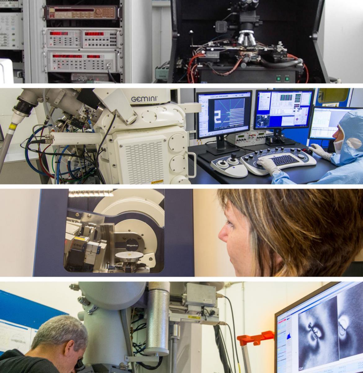
Electron microscopy
Transmission electron microscopy (TEM): Andrea Migliori
Scanning electron microscopy (SEM): Franco Corticelli
Dual beam facility: Luca Ortolani
X-ray methods
X-ray Diffraction, Reflectivity (XRD, XRR): Fabiola Liscio
Chemical methods
Gas-chromatography (GC): Stefano Zampolli
Gas sensor characterization systems: Stefano Zampolli
Contact Persons: Andrea Migliori
Instrument nameTransmission Electron Microscope FEI Tecnai F20ST
Characterizations
- Conventional TEM imaging
- Micro and nano-diffraction, electron crystallography
- High resolution (HREM) analysis
- Scanning Transmission (STEM) imaging
- Analysis of strain fields in semiconductor crystal by Convergent Beam Electron Diffraction
- Electron interferometry and holography. Measurement of mean inner potential in solids, strain in crystals, 3D structure reconstruction of curved 2D crystals, Geometric Phase Analysis
- In-situ TEM: structural and elemental analysis of samples under thermal stress, electrical stimuli and during chemical reactions in liquid environment
- EDS X-ray elemental microanalysis
- Elemental mapping in STEM mode
Technical characteristics
- Schottky emitter gun
- 200 kV max accelerating voltage
- 0.24 nm point resolution
- Scanning TEM (STEM) with BF and HAADF detector
- EDAX EDS X-ray Spectrometer
- Temperature controlled specimen holder (-180° to +100° C)
- Electron biprism for electron interferometry (home made)
- Sample holder (Protochips Poseidon) with cell for analysis of chemical reactions in liquid evironment
- Sample holder (Protochips Fusion) for TEM analysis of samples under thermal stress and/or electrical simuli
- Sample holder (home made) with electrical connections for in-situ experiments
Materials /devices to be analysed: Thin film, nanowires, nanotubes, nanoparticle and 2D systems
Samples
- Sample preparation facilities including mechanical thinning, ion milling and FIB preparation of TEM lamellae
- Ultra-microtome sample preparation
Key features/expertise
- Strong expertise in crystallography, diffraction methods, quantitative EDX, quantitative HERM, HAADF-STEM, interferometric techniques
- Development of new characterization methodologies
Relevant publications
- G. Pagot et al. Journal of Materials Chemistry A 8(48), 25727-25738 (2020)
- C. Backes et al. 2D Materials 7(2) 022001 (2019)
- G. Bepete et al. " Nature chemistry 9 (4), 347 (2017)
Contact Persons: Franco Corticelli
Instrument name
- 1. SEM Zeiss (Leo) Gemini 1530
- 2. SEM Zeiss EVO LS10
Technical characteristics
- 1. Beam energy between 0.1 and 30kV
- Schottky emitter
- InLens, Everhart&Thornley SE, BSE and STEm detectors
- X-Ray spectrometer Oxford
- Kleindiek (2) nano-manipulators adapted for in-situ low noise electrical measurements
- 2. Beam energy between 0.1 and 30keV
- Thermoionic emitter (LaB6 and W)
- Secondary and backscattered electrons detectors
- X-Ray spectrometer Bruker
- Cryo stage
- Capable to operate up to 3000 Pa with non-conductive and wet samples
Materials /devices to be analysed
- 1. Bulk, thin film, nanowires, nanotubes, nanoparticle and 2D systems
- 2. Bulk, thin film, nanowires, nanotubes, nanoparticle and 2D systems in low vacuum and environmental conditions
Key features/expertise
- Low energy STEM imaging using an optimized innovative solid-state detector for transmitted electrons developed at IMM-Bologna
- Development of an electron tomography system for the SEM composed by the in-house developed STEM detector and of an innovative eucentric sample holder fabricated for the scope
- Development of new characterization methodologies and solutions
Relevant publications
- 1.
- N. Patelli et al. Nano Energy 72, 104654 (2020)
- A. Kovtun et al. 2D Materials 6(2) 025006 (2019)
- Z.Y. Xia et al. Nanoscale 11 (12), 5265-5273 (2019)
- 2.
- G. Magnabosco et al. Materials Horizons 6(9), 1862-1867 (2019)
- D. Giuri et al. Nanoscale 11(13), 6422-6430 (2019)
- A. Busi et al. Molecular Pharmaceutics 16(3), 931-942 (2019)
Contact Persons: Luca Ortolani
Instrument name: Dual beam FIB Zeiss CrossBeam 340
Technical characteristics:
- Beam energy between 0.1 and 30kV
- Schottky emitter
- Seconday and Backscattered Electrons In-Lens Duo detector
- Secondary Ions detector
- Raith Electron Beam Lithography system
- Gas Injection System equipped with Pt, C, XeF2, SiO2 precursor for selective etching and deposition
- Kleindik (2) nanomanipulators
Materials/devices to be analysed: Bulk, thin film, nanowires, nanotubes, nanoparticle and 2D systems
Key features/expertise:
- SE and BSE imaging
- Secondary Ions imaging
- Focused Ion Beam and Focused Electron Beam micromachining and deposition
Relevant publications:C. Martella et al. Nano Research 12(8), 1851-1854 (2019)
Contact Persons: Fabiola Liscio
Instrument name: Rigaku Smartlab diffractometer
Characterizations:
- Crystal structure characterization by XRD of organic and inorganic materials (powder, thin film, multilayer, bulk)
- Stress analysis by reciprocal space map
- Texturing analysis by Pole figure
- Structural characterization at different penetration length by grazing incidence diffraction
- Morphology characterization (roughness, density, thickness, density deep profile) of thin film and multilayer
Technical characteristics:
- 5-axis goniometer (in-plane arm)
- Cu-rotating anode operating at 9kW
- Scintillator detector
- Cross beam optic to switch a Bragg-Brentato optic (for powder XRD) and a Parallel Beam optic (for thin film XRD and XRR) using a parabolic multilayer mirror
- 2xGe(220) e 4xGe(220) monochromators and 2xGe(220) crystal analyser
- X-Y sample holder for sample mapping
- Home-made sample holder for measures in operando during 1) thermal treatment (RT-300°C) in nitrogen or air, 2) during relative humidity variation
Materials/devices to be analysed: Organic and inorganic materials: bulk, thin film, nanoparticle, 2D systems, liquid and powder
Samples: Lateral size ranging from 1 mm to 10cm, possibility to scan x and y with 1/100 mm step. Sample maximum 2x2 cm2 for in situ XRD vs T.
Key features/expertise:
- Characterization of structure and morphology of condensed matter (bulk, thin film, nanoparticle and 2D systems) by means of X-ray scattering techniques, in order to be correlated with charge transport and thermoelectric properties. Strong experience in organic semiconductors (small molecules, polymers)
- Development of sample holders for in operando measurements
Relevant publications:
- XRD-GIXRD-in operando: S Milita, F Liscio, et al., J. Mater. Chem. C, 8, 3097-3112 (2020)
- XRR: F Prescimone, et al. Adv. Electron. Mater. 6, 2000638 (2020)
- XRD-in operando: C Anichini et al., ACS Appl. Mater. Interfaces, 12, 39, 44017–44025 (2020)
- HRXRD: I Bergenti, et al., J. Appl. Phys.124, 183903 (2018)
Contact Persons: Stefano Zampolli
Instrument name: GC/FID and GC/PDD
Characterizations: Analysis of liquid samples or solutions by means of gas-chromatography (GC) with flame ionization detector (GID) or pulsed discharge detector (PDD).
Technical characteristics:
- Thermo Scientific FocusGC and TraceGC instruments
- Split/splitless injector
- Flame ionization detector
- He pulsed discharge detector
Materials /devices to be analysed: Solutions of volatile and semi-volatile species. FID is suitable for hydrocarbons while PDD can be used for a broader range of substances.
Samples: Lateral size ranging from 1 mm to 10cm, possibility to scan x and y with 1/100 mm step. Sample maximum 2x2 cm2 for in situ XRD vs T.
Key features/expertise Use of benchtop laboratory GC systems for the characterization and optimization of MEMS analytical devices: use of innovative MEMS-based injectors, MEMS GC columns, MEMS detectors.
Relevant publications
- A. Hackner, et al., Sensors and Actuators, B: Chemical 185, 771-776 (2013)
- F. Rastrello, et al., IEEE transactions on instrumentation and measurement 62, 974-981 (2013)
Contact Persons: Stefano Zampolli
Instrument name: Custom made gas sensor characterization systems 1-3
Characterizations: Exposure of gas sensors and gas sensing systems to known mixtures of gases from certified cylinders.
Technical characteristics:
- Up to 10 mass flow controllers for mixtures of 8 gases + humidity
- Software-controlled complete automatization
- Possibility to generate and log random mixtures
- Three different gas sensor benches available
Materials/devices to be analysed: Gas sensors and gas sensing systems requiring sample flows up to 500 mL/min.
Key features/expertise:
- All gas sensor characterization systems are custom made in house and can be adapted/modified for specific characterization applications. Automation software can be reconfigured for execution of lists or random mixtures with logfile.
- Capabilities for post-process scripting and combination of sensor data and random mixture generation logs to extract training and test patterns for AI.
Probe stations for AC/DC/pulsed measurements: Luca Belsito
Hall measurement system: Luca Belsito
Electro-chemical method: Raffaello Mazzaro
Contact Person: Luca Belsito
Instrument name: Probe-Stations for AC/DC measurements
Characterizations: the electrical lab for device testing is equipped with 6” and 12’’ probe stations and related rack for DC and AC testing:
- MICROMANIPULATOR P300A Semi-Automatic Probe Station
- MICROMANIPULATOR 6600 Probe Station
- Keysight B1500A Semiconductor Device Parameter Analyzer with fours SMU;
- Digital Oscilloscope LeCroy 6100 oscilloscope;
- 238 High current source measure units (4 instruments)
- Network e spectrum analyzer MS2036C
Technical characteristics:
- Current-voltage (IV) measurement capabilities in the range 0.1 fA - 1 A / 0.5 µV - 200 V
- AC capacitance measurement from 100 Hz to 2 MHz
- S-Parameter Measurements from 5 kHz to 6 GHz
Materials/devices to be analysed: Diode, transistors, MEMS
Samples: Devices from 1x1 cm2 to 12”
Key features/expertise: Characterization of electronic devices and microsystems. Dedicated software developed in-house with Labview for custom measurements
Relevant publications: L. Belsito et al., Sensors and Actuators, A: Physical, 239, pp. 90–101 (2016)
Contact Person: Luca Belsito
Instrument name: Hall effect
Characterizations Hall measurements (1T magnetic field strength) performed by:
- BRUKER RESEARCH MAGNET B-E 10 C8
- EA-PS 9200-25 T Power supply
- KEISIGHT 34358A Multimeter
- KEITHLEY 220 PROGRAMMABLE CURRENT SOURCE
- KEITHLEY 220 705 SCANNER
- MMR K-20
Technical characteristics: Hall and resistivity measurements in the range 25-380 °C
Materials/devices to be analysed: Semiconductors
Samples: 1 x 1 cm2 sample holder for Resistivity and Hall mobility measurements in Van der Pauw and Hall bar geometries
Key features/expertise: Dedicated software developed in-house for Resistivity and Hall measurements
Relevant publications
- R.Nipoti et al., Materials Science Forum, Volume: 1004 Pages: 698-704 (2020)
- R. Nipoti et al., Materials Science Forum, Volume: 1004 Pages: 683-688 (2020)
Contact Person: Raffaello Mazzaro
Instrument name: Potentiostat/galvanostat/ZRA Reference 600+ Gamry
Characterizations:
Technical characteristics:
Materials/devices to be analysed: Physical electrochemistry and Photoelectrochemistry of solution-based compounds and nanostructured thin films.
Samples: 1 x 1 cm2 sample holder for Resistivity and Hall mobility measurements in Van der Pauw and Hall bar geometries
Opto-electronic and spectral analysis
Infrared, visible, UV
Fourier-Transformed Infrared Spectroscopy (FTIR): Caterina Summonte
Ultraviolet-Visible-near Infrared Spectrophotometry (UV-Vis-NIR) Caterina Summonte
Contact Person: Gabriele Bolognini
Instrument name: Opto-electronic and spectral analysis test-bench
Characterizations: Complete opto-electronic and optical fiber characterization, in particular:
Technical characteristics:
Devices to be analysed:Fiber-based and open-space optical sources and devices
Key features/expertise: Bench with all the equipment required for the characterization, evaluation and monitoring of relevant properties (such as polarization, intensity, frequency spectrum) of opto-electronic devices, alongside the monitoring of integrity for fiber-based system.
Relevant publications:
Contact Persons: Gabriele Bolognini
Instrument name: Distributed optical fiber sensing device bench
Characterizations:
Technical characteristics:
Devices to be analysed: Distributed temperature and strain sensing, temperature/strain sensing fibers evaluation, data and signal processing techniques
Key features/expertise:Bench with different distributed optical fiber sensors for studying optical, electronic and data processing methods for improved temperature, strain and spatial resolution, evaluating de-noising techniques, characterizing noise sources and testing sensing fibers.
Relevant publications:
Contact Person: Caterina Summonte
Instrument name: Thermo Nicolet
Technical characteristics: Spectral range: 400 - 12000 cm-1; spectral resolution 4 cm-1
Materials/devices to be analysed: Thin film thickness analysis and anti-reflection coating analysis; analysis of novel nanocomposite materials.
Samples: Solid, minimum size 0.5 cm x 0.5 cm.
Excellence:Optical response of dielectric thin films, dopants in Si.
Contact Person: Caterina Summonte
Instrument name: HP8452A Diode array / Avantes fiber optics
Technical characteristics:
Materials/devices to be analysed: Thin film thickness analysis and anti-reflection coating analysis; analysis of novel nanocomposite materials; color measurements and matching; optical density measurements (e.g. optical filters and safety eye wear); Spectral measurements.
Samples: Solid, minimum size 0.5 cm x 0.5 cm.
Excellence:Optical response of dielectric thin films, dopants in Si.
Contact Person: Caterina Summonte
Instrument name: HP8452A Diode array / Avantes fiber optics
Technical characteristics:
- HP8452A Diode array spectral range: 190-820 nm (resolution 1 nm)
- Avantes fiber optics spectral range: 250 - 1100 nm (resolution 0.314 nm at 633 nm)
Materials/devices to be analysed: Thin film thickness analysis and anti-reflection coating analysis; analysis of novel nanocomposite materials; color measurements and matching; optical density measurements (e.g. optical filters and safety eye wear); Spectral measurements.
Samples
- Solid: minimum size 0.5 cm x 0.5 cm
- Liquid: to be discussed
Excellence: Study of the optical response of 2D materials and thin film oxides.
Contact Person: Caterina Summonte
Instrument name: ORIEL and home made systems
Technical characteristics:
- Quantum efficiency of solar cells
- J-V characteristics of solar cells
- AM1.5 global
- 375 - 1100 nm (set of BP filters)
- JV, I(T), -20 to 250°C
Materials/devices to be analysed: optical characterization of photovoltaic devices, electrical characterisation of pv devices and amorphous semiconductors
Samples
- Solid: minimum size 0.5 cm x 0.5 cm
- Liquid: to be discussed