
The long standing experience on the synthesis of materials for electronic applications of IMM Bologna has been devoted to the development of different CVD type of equipment and methodologies for the synthesis of advanced materials. Recently, this activity has been mainly focused on the study of the synthesis of low-dimensional materials, such as high quality C nanotubes, mono and few-layer graphene and graphene foams, Si nanowires and nanoparticles, Si nanocrystals embedded in SiC thin films, nanometric SiN or SiC based multilayers. Transparent conductive metallic oxides, metallic catalytic nanoparticles and other standard thin films for microelectronics has been synthesized using PVD techniques.
Laboratories in the Clean Room environment (class 100 and 100000):
1) CVD systems laboratories
2 Hot-Walls CVD systems: 2” quartz tubes, T up to 1000 C, (3x6) cm2 flat samples or (7x6) cm2 Cu foils and 1 Cold-Walls CVD System (Elettrorava – IMM-Bo): T up to 900 C, 3-4” flat substrates, base vacuum < 10-7 mbar, heater under a quartz bell separately evacuated down to 10-7 -10-8 mbar, fully computer controlled. These reactors are dedicated to the controlled synthesis of C-based nanostructures such as C nanotubes on different substrates (both vertically and horizontally aligned), high quality mono and few-layer graphene and graphene foams.
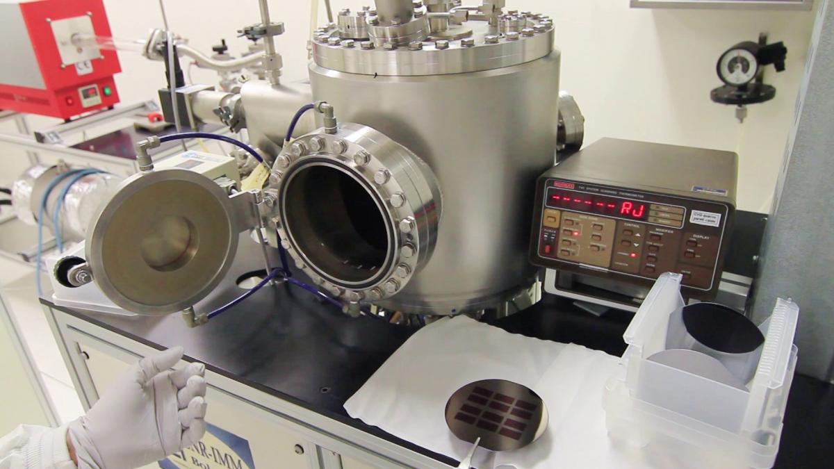
Cold-wall C-CVD system dedicated to the synthesis of C-based nanomaterials
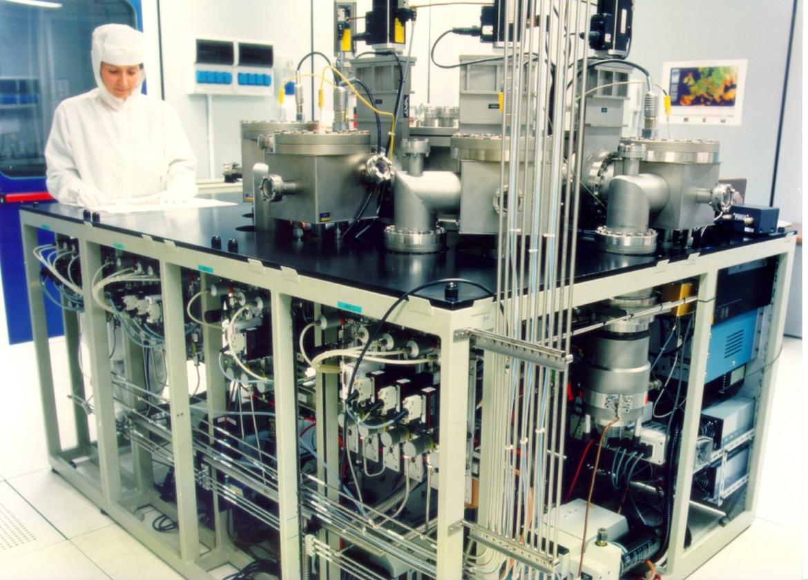
1 RF – VHF multi-chamber PECVD system (Elettrorava – MVSystem): (10x10) cm2 substrates, 4 chambers, separate turbomolecular pumping (10-8 torr), 13.56 to 100 MHz, plasma ignitor, fully computer controlled. This system is dedicated to the synthesis of Si-based intrinsic and doped amorphous and nanocrystalline films (a-Si:H, a-SiC:H, a-SiN:H, nc-Si and nc-SiC), SiC or SiN based multilayers, p-i-n and similar devices for applications in Photovoltaics and Optoelectronics (heterojunction solar cells, thin films solar cells on nanostructured back reflectors, optical modulators)..
2 horizontal LP-CVD systems SEMCO Minilab DF 500-6 dedicated to the deposition on 6” wafers of LTO from SiH4 and of SiO2 from TEOS source
2 horizontal LP-CVD systems ASM 185-2, for the deposition on 4” wafers of Si3N4 and poly-Si.
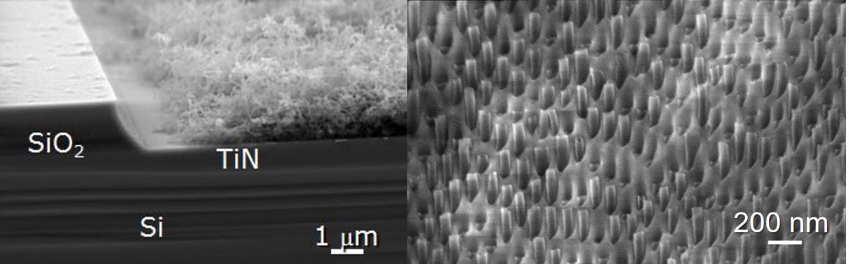
Carbon nanotubes on-site grown in an SiO2 well (left) and inside tha nanopores of an Al2O3 matrix (right).
2) PVD systems laboratory
2 RF magnetron sputtering systems: MRC8603 (3 magnetron 6.5” cathodes) and MRC8622 (2 diode + 1 magnetron 6” cathodes) with DC and RF generator, for the deposition of thin and ultrathin metallic films, TiN, SiO2 Al2O3, TiO2 and other metal oxides.
1 e-beam evaporator VARIAN 3119 for the deposition of thin and ultrathin metallic films and oxides.
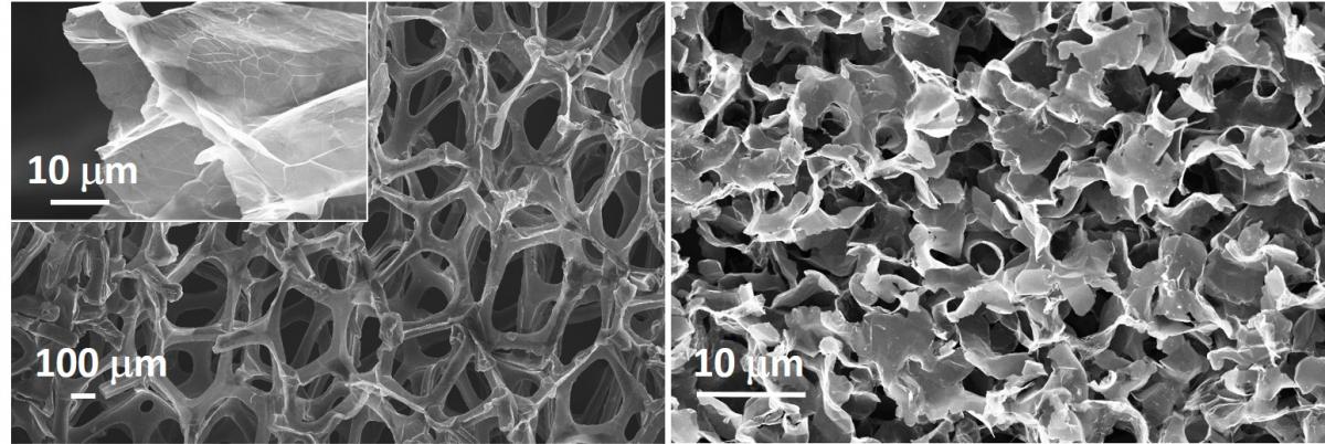
Graphene foams of varying density obtained by using Ni (left) or Ni nanoparticles foams (right)
Outside the Clean Room environment:
1 RF magnetron sputtering system (custom-made, 2 magnetron 4”cathodes) for the deposition of ITO, AZO, IWO.
Tubular furnace for the synthesis of Si nanoparticles by high temperature annealing of HSQ in Ar + H2: T up to 1600°C - controlled over 3 regions, atmospheric and low pressure processes, 3” substrates, fully computer controlled processing.
Contact person: Rita Rizzoli