
| Growth/Deposition Processes |
| PROCESS | LAYER | THICKNESS RANGE | TOLERANCE |
| Furnace Treatments | SiO2 (Wet process) | 10-1500 nm | 5% |
| SiO2 (Dry process) | 10 - 300 nm | 5% | |
|
Low Pressure Chemical Vapor Deposition(LPCVD) |
Poly-Si | 30-3000 nm | 5% |
| LTO (stress free) | 20-5000 nm | 5% | |
| Si3N4 | 20-400 nm | 5% | |
| TEOS | 20 - 2000 nm | 5% | |
| Plasma Enhanced CVD (PECVD) | a-Si:H, a-SiC:H, a-SiN:H, nc-Si, Si3N4 | 0-4 µm | 4% |
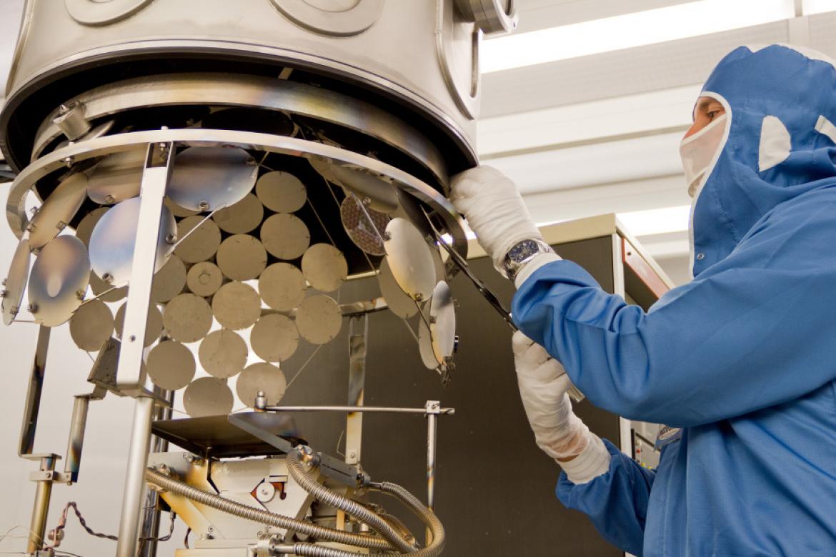
| Sputtering | Sn, Pt, Au, TiN, SiO2, Al-1% Si, Ti | 3nm - 2µm | 10% |
| Electron beam evaporation | Al, Ti, Ag, Mo, Ni, Cr, Pt, Pd, Co, Fe, SiO2 | 3nm - 2µm | 3% |
| CVD for carbon nanotubes and graphen-based materials | MWCNTs, SWCNTs, nanopipes in nanoporous templates, nanowires, graphene films on Cu substrates, graphene foams on metallic (Ni, Steel) prous substrates | 500 μm | - |
| Controlled anodic oxidation | Nanoporous Al2O3 templates (pore diameter 40-100 μm, pitch 100-500 μm) | 5-500 μm | - |
| Thermal Processes |
| Process | Material | Annealing Time | Annealing Temperature |
| Phosphorus doping | Si | 10 min-1 h |
from 920 °C up to 1000 °C |
| Furnace anneal | Si, SiC | 5 min-60 h |
|
| Rapid Thermal Annealing (RTA) Lamp | Si, SiC, Ge | 1s - 5 min ramp up to 250°C/s |
250 -1100°C |
| Ultra High Temperature annealing (UHT) RF | Si, SiC (max 2inch substrate) |
1 -60 min |
750- 2000°C |
| Photolithographic Processes |
| Process | System | Mask Plate / Wafer Size |
Minimum Feature Size |
| Vapor Prime | HMDS Hotplate | piece up to 4 inch | |
| Photoresist Deposition | Spin-coat | piece up to 4 inch | |
| Photoresist exposure | Front Side aligner Deep UV (250 nm Wave length) | 2-4 inch | 600 nm |
| Front-to-back side aligner Near UV (400 nm Wave length) | 2-4 inch | 1.25 µm | |
| Baking | Hot Plate up to 300 °C | piece up to 4 inch | |
| Hot Plate with controlled rampe up to 300 °C | piece up to 4 inch |
| Etching Processes |
| Process | Layer etched | Chemistry | Rate |
| Reactive Ion Etching (RIE) | SiO2 | CHF3/Ar | 30 nm/min |
| Si3N4 | CHF3/Ar | 20 nm/min | |
| Si | SiCl4 SF6/O2 |
60 nm/min 1.0 µm/min |
|
| Poly-Si | SiCl4 | 60 nm/min | |
| SiC | SiCl4/Ar/O2 CHF3/Ar/O2 |
38 nm/min 27 nm/min |
|
| Al | BCl3/Cl2/Ar | 50-100 nm/min | |
| Deep Reactive Ion Etching (D-RIE) | Si | SF6/C4F8 | 1-13 µm/min |
| SiO2 | C4F8/He/CH4 | 0.4 µm/min | |
| Plasma stripper | Photoresist | O2 | >100 nm/min |
| Ion Implantation Processes |
|
Process |
Implanted Species | Energy Range | Temperature |
| High Energy | H, He, B, N, O, Al, Si, P, As | 500-5000 keV | -60 - 700 °C |
| Wafer Bonding Processes |
| Process | Substrate material | Substrate # |
| Anodic | Si, Pirex | 2 - 3 |
| Fusion | Si | Up to 3 |
| Glass Frit | Si, Pirex, other | 2 |
| Eutectic | Si | 2 |
| SIO | Si, SiO2 | 2 |