Currently employed electronic interconnection networks are reaching their limits in terms of bandwidth, wiring density, and power consumption. Therefore to avoid an exponential growth of dissipated power, the power efficiency must be increased in next-generation high-end servers and computing systems. The problem of reaching physical limits in power density and backplane interconnections is a compelling issue also for standard Internet communications posing serious reliability concerns due to the large amount of active components.
To counteract these problems, the introduction of optics in interconnects and switching fabrics has the potential to scale to higher capacities, reduce the power consumption, and increase the reliability bringing down costs.
Microring resonators constitute the basic building blocks for optical switching. They are studied and fabricated on different Silicon On Insulator (SOI) based technology which is fully CMOS compatible, thus allowing a complete integration between the electronic boards and the optical network.
The technological schemes proposed in literature involve both static and dynamic ring resonator-based switches, each of them having specific features, and both are suffering from limitations that cannot be overcome with existing technologies. In fact, the resonance wavelength tuning has been achieved, according to state of the art, basically using two different effects: the thermo-optic effect and the electro-optic effect through carrier injection. The first effect allows larger resonance shifts (and therefore larger tunability), but is characterized by a slow response time (exceeding the millisecond value), hindering the possibility of dynamic switching. The second effect (carrier injection) is inherently faster (switching times down to microsecond order and smaller), but suffers from very high carrier-induced optical propagation losses (exceeding 100 dB/cm) depending on injected current, thus also limiting the usage to small wavelength shifts. Both effects exhibit non-negligible power consumption, due to resistive heating for thermo-optic effect or related to current propagation for carrier injection technique.
A novel alternative way to induce the electro-optic effect (Pockels effect) in silicon can be exploited by employing a straining film deposited onto the device. The electro-optic coefficient generated in this way, as observed in very recent literature discussed in the state-of-the art section, potentially allows for very fast switching speeds (as with carrier injection solutions), together with large wavelength shifting capability (as with thermo-optic effect). Furthermore, an overall negligible power consumption can be expected, since exploiting Pockels effect requires only a generation of an electric field, without appreciable current flow through the devices contacts, thus resulting in a significantly higher power efficiency. Moreover, strained silicon technology is expected to be less expensive compared to carrier injection based techniques due to a significantly lower number of processing steps.
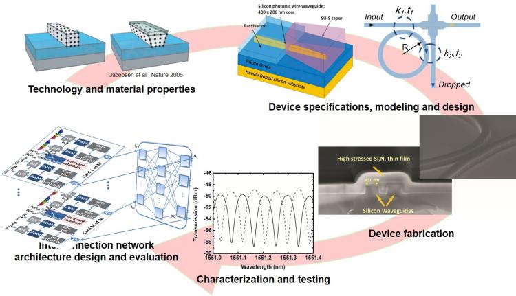
The building block of the proposed switching devices is sketched in Fig. 1 and essentially consists of a microring integrated on a dielectric substrate where the light is injected and coupled out by two coupled submicron silicon waveguides placed close to the resonator.


