
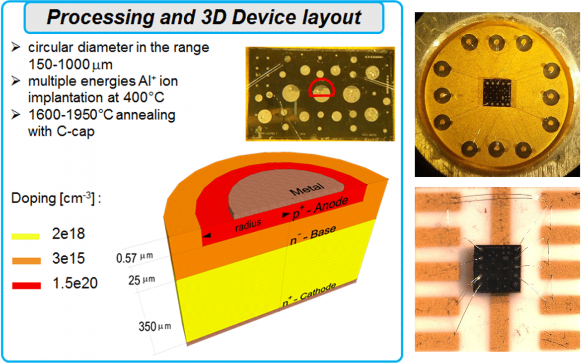
IMM of Bologna studies the optimization of the electrical doping of single crystal 3C- and 4H-SiC poly-types by ion implantation. When the fabrication of SiC electronic devices is concerned, the optimal electrical doping is a compromise between the desired electrical activation of the implanted dopant species and the achievement/preservation/restoration of the best reachable current transport and/or blocking voltage features of the device under fabrication. To be able to fix this compromise before device processing a very good knowledge of the electrical activation process is necessary. At the same time it is necessary to gain a very good knowledge of the collateral effects that the mandatory post implantation annealing treatment for the electrical activation of the ion implanted species, may have on the carrier transport features. IMM-Bologna is working for reaching both the knowledge with the aim to exploit them in SiC device demonstrator at TRL3/4.
For a long time, the post implantation annealing time of SiC has been considered of minor relevance with respect to the annealing temperature and the implanted dopant concentration because of trends like that shown in Fig. 1 where the sheet resistance (resistivity) is use as a benchmark of the electrical activation of ion implanted Al in 4H-SiC [Nath et al., J. Electron. Mater. 43, 843 (2014)].
|
|
Fig. 1. Room temperature (RT) resistivity of Al+ implanted 4H-SiC layers after annealing tretament at different temperatures from 1650 °C to 2100 °C. Implanted Al concentrations was homogeneous in the range 1017 - 3 x 1021 cm-3. Implantation temperature was in the range 300-600 °C. CA stays for conventional annealing, and MWA for microwave annealing. Anneling time ranges from 5 to 30 min in the case of CA, and was 0.5 min in the case odf MWA. The dominant trend is a decreasing of the implanted p-type 4H-SiC with the increasing of the post implantation annealing temperature.
|

When the attention has been addressed to the post implantation annealing time, results like those of Figs. 2 have been obtained [Nipoti et al., Mater. Sc. Forum, 924 (2018) 333-338]. The extremely long time for reaching the saturation of the electrical activation at temperatures lower than 1700°C and the correspondent minimum time of 30 min for temperatures higher and equal to 1700°C, arise the item of the control/knowledge of the electrical activation kinetics in ion implanted 4H-SiC. The latter a subject of research not yet afforded for SiC, to the best of our knowledge.
|
|
Fig. 2. Sheet resistance and resistivity values at 25 °C in a 1×1020 cm-3 Al+ ion implanted 4H-SiC layer after annealing with S&S and F&F in ABB and IMM furnaces. S&S means “heating and cooling rate < 100°C/s”. F&F means “heating and cooling rate > 100°C/s”. ABB and IMM stay for industrial and research furnace, respectively. Correspondences between symbols and processing are shown in the inset. Data errors are of the order of 15%. Dashed lines are for guiding the eyes. The good overlap between ABB and IMM data prove that a technological transfer of the optimized receipts in the IMM furnace can be performed towards the ABB one. |

The equilibrium concentration of the life time killer defect carbon vacancy (VC) in the drift regions of SiC devices were expected to be mostly affected by the post implantation annealing temperature than C atom injection from the SiC ion damaged layer when temperature values above 1400°C are used [Ayedh et al., J. Appl. Phys., 118, 175701 (2015)]. Fig. 3 and 4 confirm such expectation. In fact, vertical p-i-n diodes fabricated by ion implantation on the same n-type epitaxial 4H-SiC wafer with emitters of different ion implanted Al concentrations show longer carrier life time (measured by Open Circuit Voltage Decay) and VC concentration below the detection limit of DLTS (Deep Level Transient Spectroscopy) when annealed at 1650°C with respect to when they are annealed at 1950°C [Nipoti et al, Mat. Sc. Forum, 897 (2017) 439-442, Nipoti et al., Materials Science in Semiconductor Processing, 78 (2018) 13-21]
|
Fig. 3. OCVD (Open Circuit Voltage Decay) measurement of Al+ ion implanted 4H-SiC p-i-n diodes with different post implantation annealing processes: (red line) 1600 °C/30 min with of 694 ns OCVD life time and (blue line) 1950 °C/5 min with 164 ns. Higher annealing temperatures correspond to shorter carrier life times. |
Fig. 4. DLTD spectra of the Al+ ion implanted vertical diodes of Fig. 3. Diode A (red line) is 1600°C/30min annealed while Diode B (blue line) is 1950°C/5min. VC are under the detection limit in the case of diode A. Details of DLTS measurements can be found in [Nipoti et al., Materials Science in Semiconductor Processing, 78 (2018) 13-21]. |


Contact person: Roberta Nipoti