
CLEAN ROOM ISO 5 (100 CLASS)
INTRODUCTION
| Individually or in combination with e-beam lithography, the SCILL NIL system can be used for large-area device nanofabrication. Nano Imprint Lithography (NIL) is an emerging lithographic technology that promises high throughput patterning of nanostructures. With NIL it’s possible to achieve sub-50nm resolution features over large areas. NIL can significantly simplify the production of nanostructures using a wide variety of materials. NIL intrinsically has better dimensional control that can be achieved using conventional UV lithography |
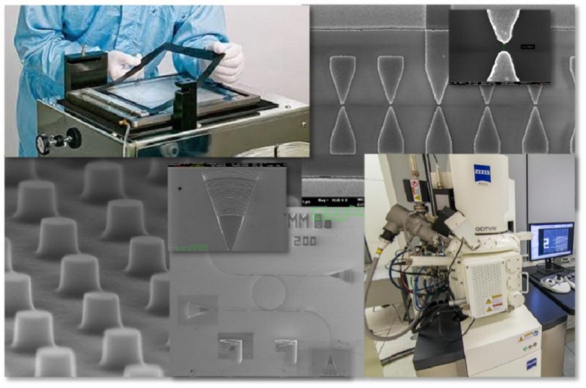
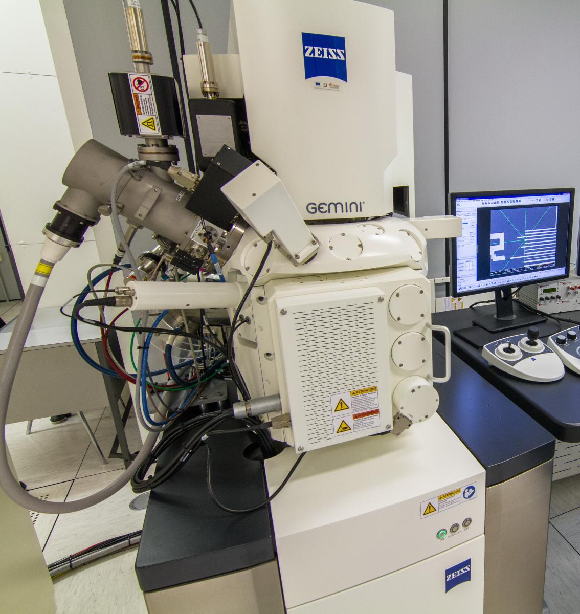
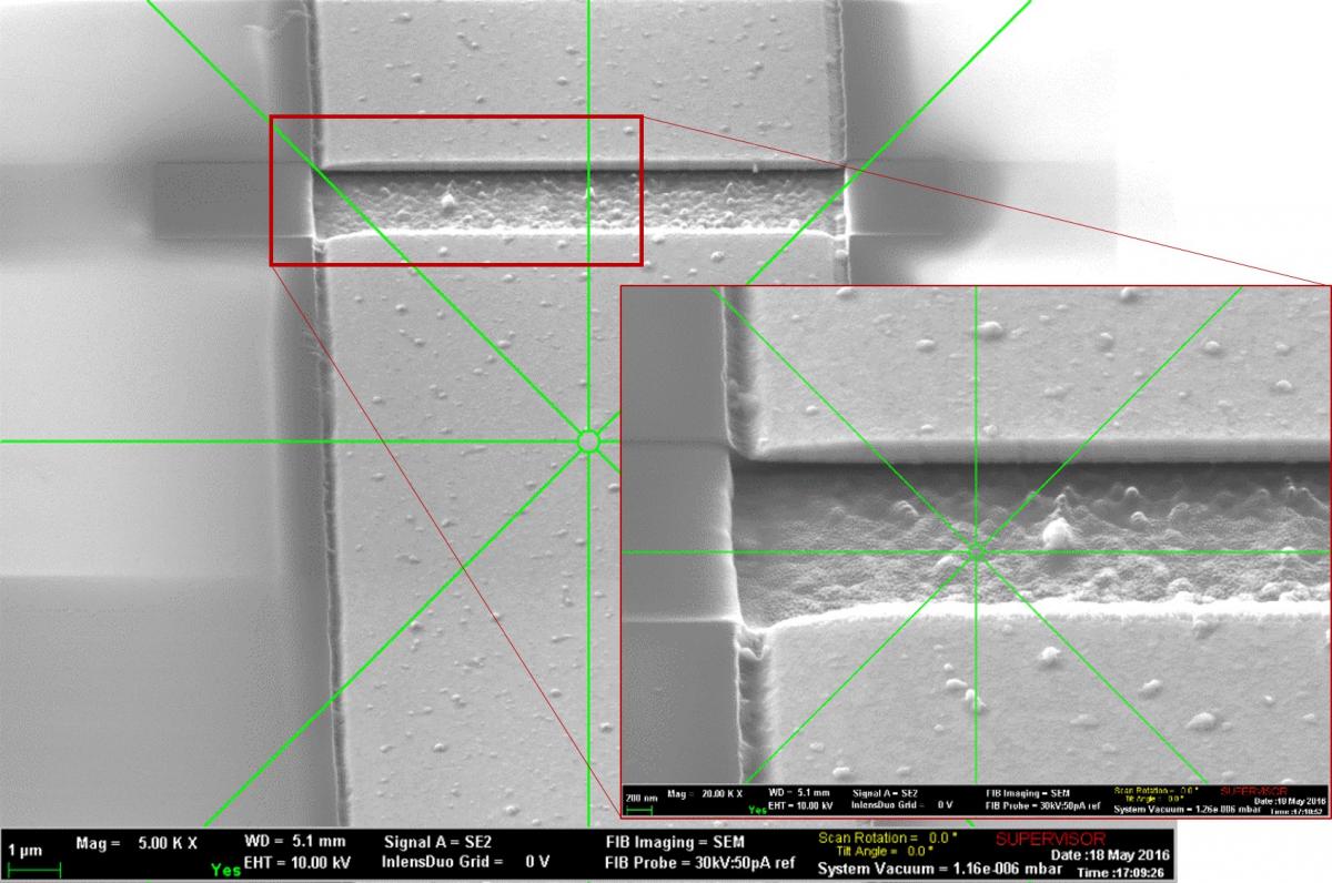
| Dual beam FIB Zeiss CrossBeam 340 | |
|
|
The CrossBeam 340 dual beam facility has a Gemini FEG electron column and a Ga ion column and is equipped with a gas injection system, a Raith Elphy Quantum nanolithography attachment and Kleindiek micromanipulators. This instrument is located in clean room environment. (Dr. I. Elmi) This instrument allows operation at micro-nanometric level, which includes (but not limited to):
|
| CONTAC PERSON: IVAN ELMI | |
| TECHNICAL SPECIFICATIONS: | |
|
Scanning Electron Microscope (SEM) Features
Electron Beam Lithography (EBL) Features |
Gas Injection System (GIS) Features Focused Ion Beam (FIB) Features |
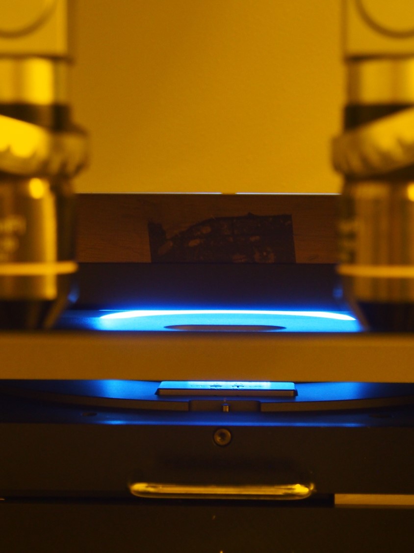
| UV- IMPRINT LITHOGRAPHY | |
|
|
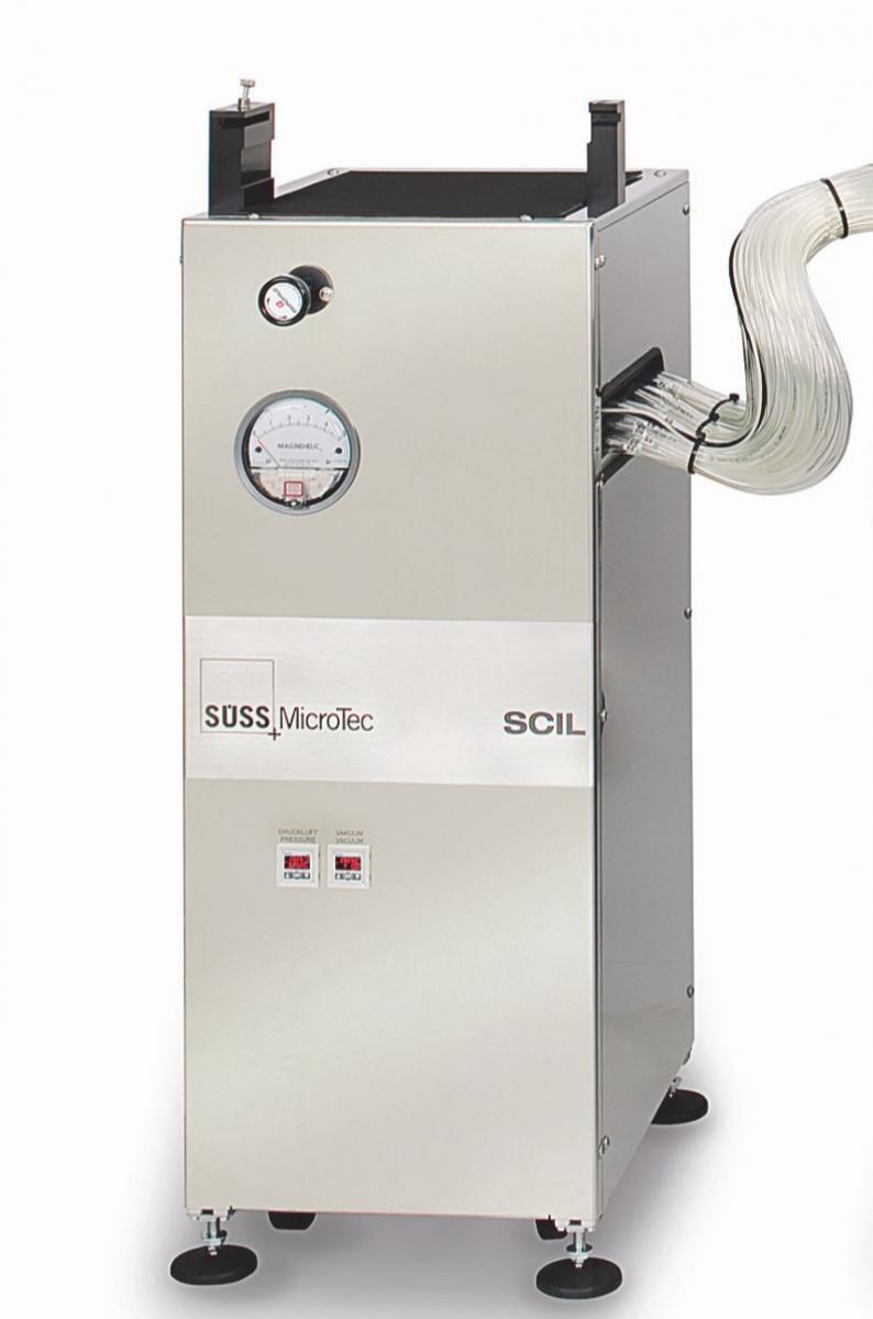
SUBSTRATE CONFORMAL IMPRINT LITHOGRAPHY (SCIL) UV-NIL is a low-cost production technology based on UV-curing. It has been developed as a costeffective alternative to high-resolution e-beam lithography to print nanometer sized geometries. TECHNICAL SPECIFICATIONS:
|
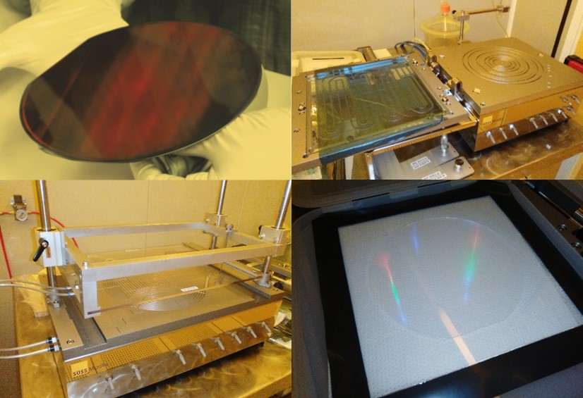
| REPLICATION TOOS FOR SOFT-MASTER NANOIMPRINT | |
|
|
SCIL STAMP REPLICATION The Substrate Conformal Imprint Lithography (SCIL)technique bridges the gap between UV-NIL with rigid stamp for best resolution and soft stamp for large-area patterning. SCIL uses a sequential imprinting principle that is based on capillary forces The Master Replication Tooling (MRT)
The SUSS Peel-Off Tooling (POT) |
| CONTACT DEEP UV PHOTOLITHOGRAPHY | |
|
|
|
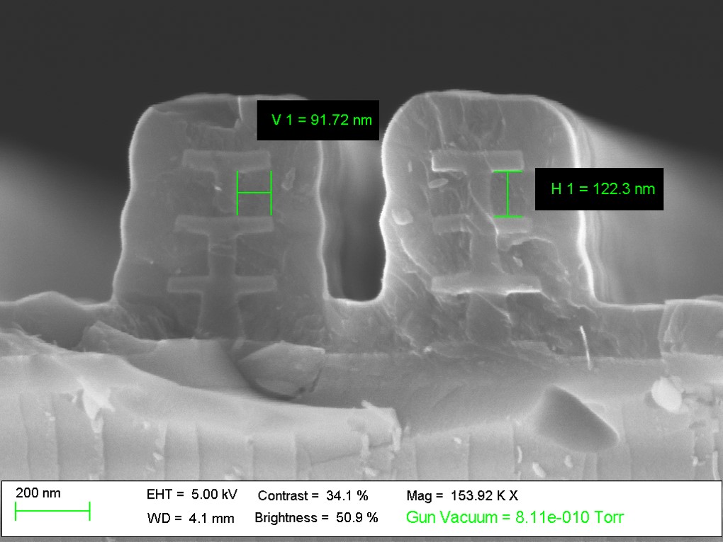
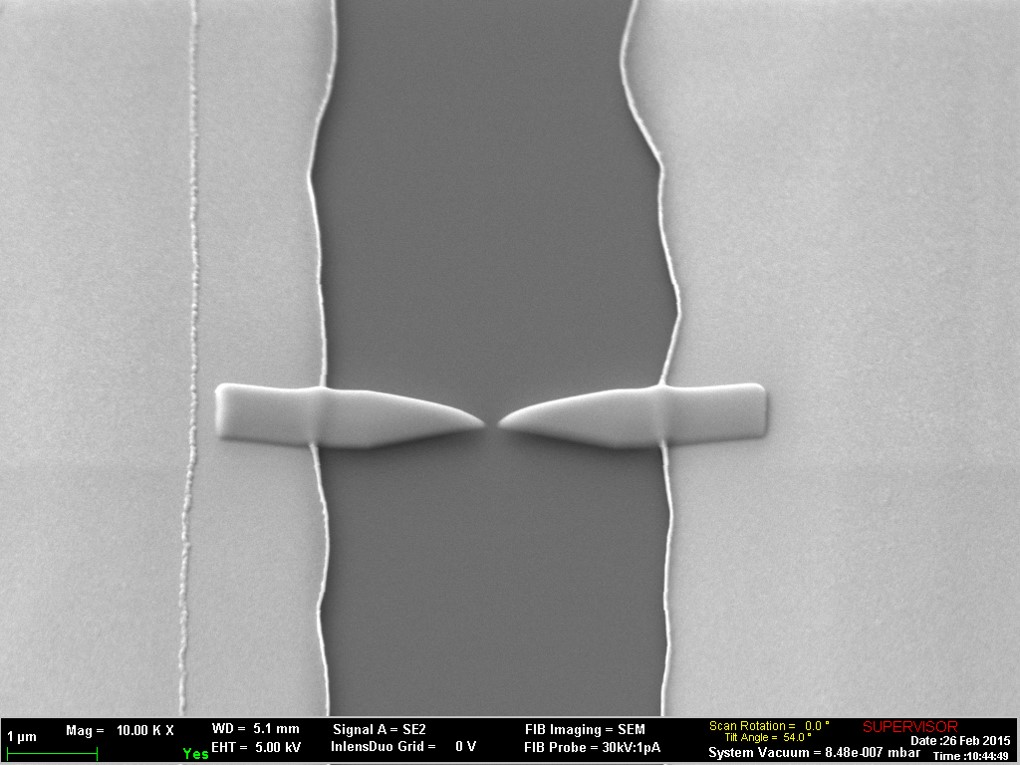
| MULTILEVEL POLYSLICON NANOWIRES MANUFACTURED BY DEEP UV PHOTOLITHOGRAPHY AND SPACER TECHNOLOGY | FIB CROSS-SECTIONING OF A SUBMICRON SILICON WAVEGUIDE |
|
|
|
|
|
|

PROCESSES AVAILABLE
| MICRO/NANO FABRICATION HOME PAGE |