
INTRODUCTION
|
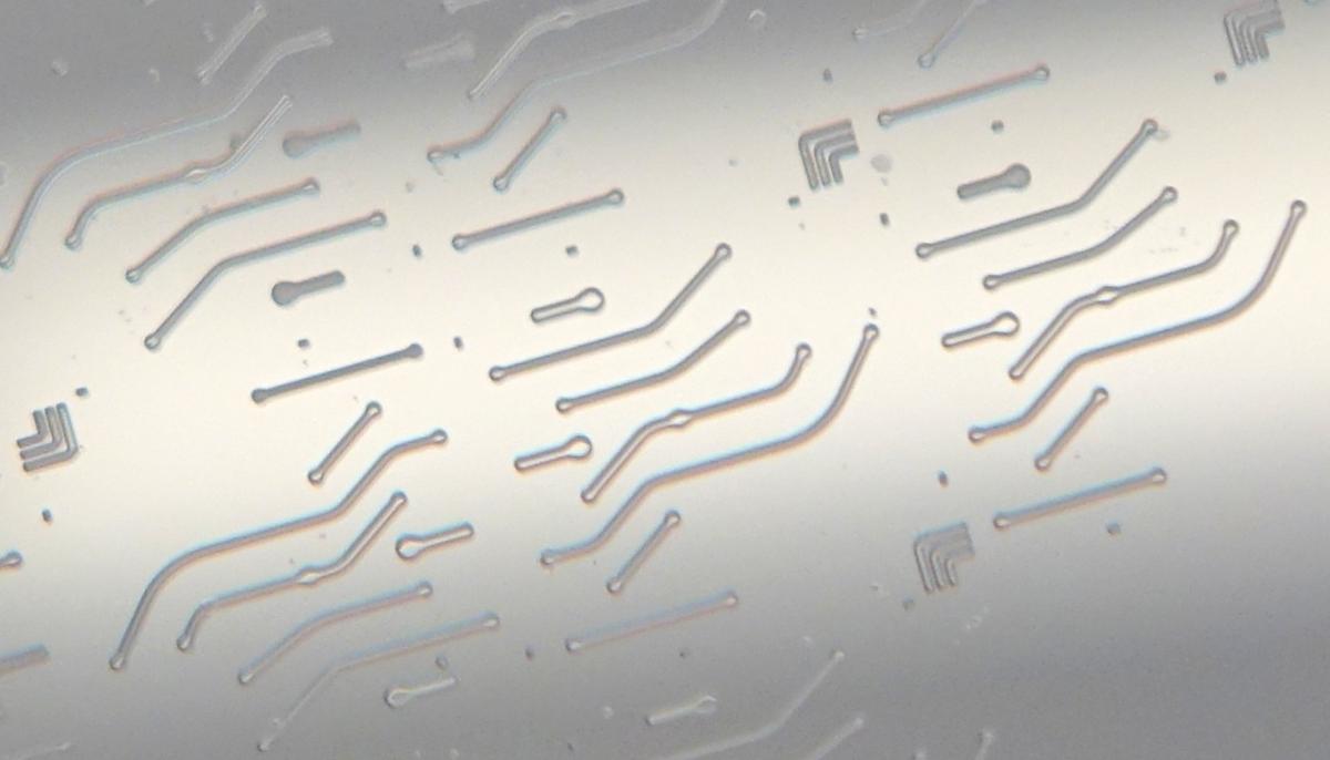
The Microsystems Laboratory is a semiconductor processing facility specializing in the fabrication of various types of chemical, physical sensors and multifunctional microsystems. The facility consists of more than 50 m2 of Class 100 (ISO 5) clean room space. Process capabilities Deep plasma etching, wet anisistropic silicon etching, deep glass wet etching and wafer bonder. The microsystem laboratory works in synergy with all the other laboratories |
EQUIPMENT
| WET BENCH FOR TMAH/KOH | |
|
|
Chemical wet bench to fabricate high aspect ratio silicon structures. The systems allow the wet etching with alkaline solutions (KOH, TMAH) of
|
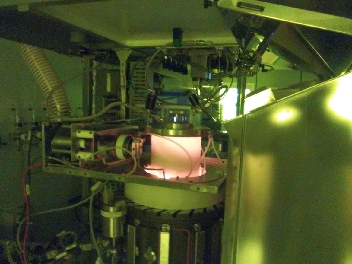
| DEEP REACTIVE ION ETCHING | |
|
|
DEEP REACTIVE ION ETCHING ALCATEL A601E
Using deep reactive ion etching (DRIE), high aspect ratio trenches can be etched in silicon with near-vertical sidewalls. With an etch depth more than 500 µm, hole diameters of greater than 50 µm are feasible. This technology module is used, for example, in the manufacturing of silicon accelerometer, or gas crhomatographic coloumn |
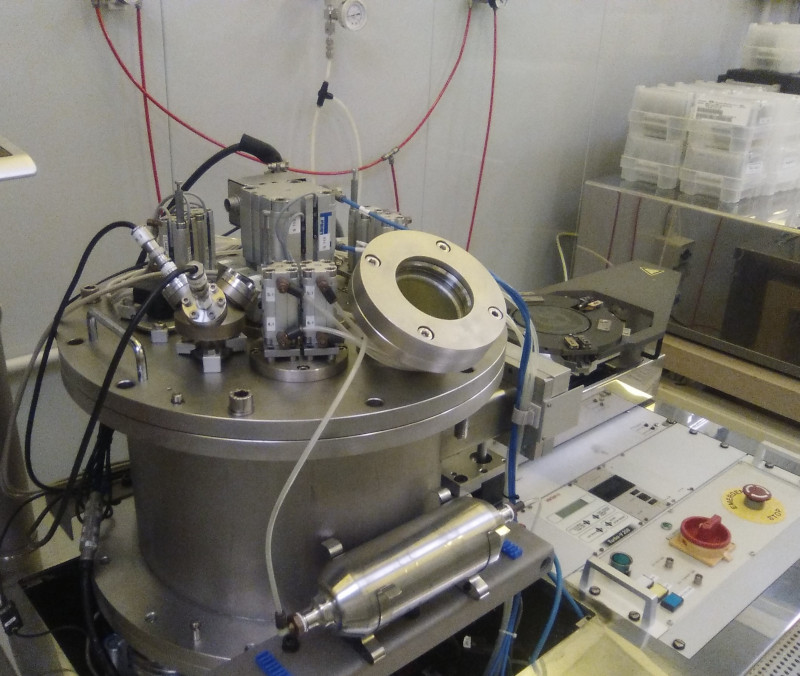
| WAFER BONDER | |
|
|
WAFER BONDER SB6 SuSS Microtec
WAFER ALIGNER BA6 SuSS Microtec
|
| GLASS AND FUSED SILICA DEEP ETCHING | |
|
|
Glass wafers are commonly used in micro-devices due to their excellent mechanical and optical properties. The wet etching of the glass wafer is widely used during the fabrication of micro-devices. Cr/Au hard mask is also a commonly used masking material due to the inert property of gold when in contact with concentrated HF (49%) |
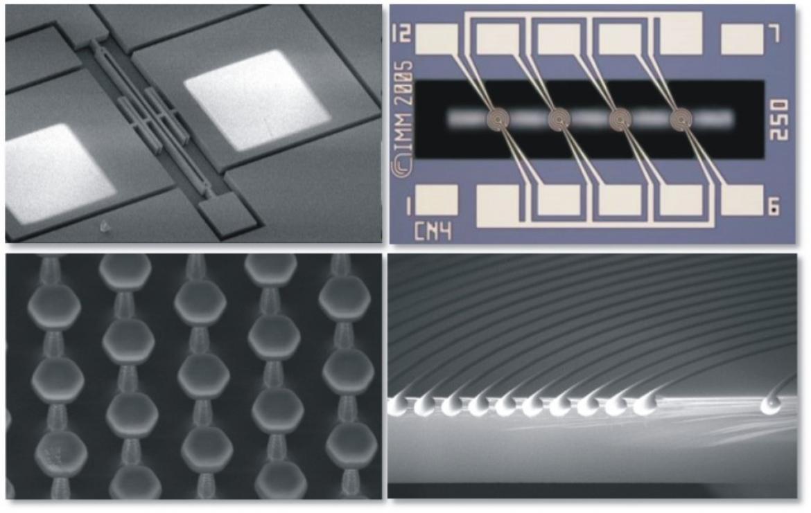
AVAILABLE TECHNOLOGIES
AVAILABLE PROCESSES
FOR MORE INFORMATION:
| MICRO/NANO FABRICATION HOME PAGE |