Primary tabs

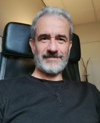
Roberto Balboni is Researcher at the Bologna site of CNR-IMM Institute. He graduated in Physics at the University of Bologna in 1988 and his research activity has been devoted to the characterization of materials mainly using electron microscopy methods, but also by means of X-rays diffraction. He was at Department of Physics of the University of Modena until 1993, where he used scanning and transmission electron microscopy and microanalysis to characterize semiconductor materials and devices. In 1984 he moved to CNR-IMM (formerly LAMEL Institute) where, in addition to electron microscopy, he also worked on X-ray diffraction characterization and modeling in semiconductor and on electromigration issues in metal interconnects. At CNR-IMM he developed the use of convergent beam diffraction analysis to study strain fields at the nanoscale in crystalline materials, by setting up both the experimental procedure and the theoretical modeling and computer code. He participated to the project STREAM (FP5), funded by the EC and coordinated by CNR-IMM Bologna, to set up the procedure and codes for strain analysis in semiconductor structures and devices.
He was responsible for the CNR participation in the project ANNA (FP6), funded by the EC.
He authored more than 80 papers in international journals presented his work on more than 70 international conferences.
He was in the Scientific committees of several international conferences on Microscopy.
He was Director of five editions of the TEM School in Materials Science in Bologna from 2008 to 2016.
He is presently President of the Italian Society for Microscopical Sciences.
Scientific Production
Intelligent Computing [AAAS], Volume: 2022 Pages: 0001
Enhancing Electron Computational Ghost Imaging Using Artificial Neural Networks
Microscopy and Microanalysis [Cambridge University Press], Volume: 28 Issue: S1 Pages: 2242-2244
Computational ghost imaging for transmission electron microscopy
arXiv preprint arXiv:2204.09997 [],
Journal of Applied Physics [AIP Publishing LLC], Volume: 131 Issue: 3 Pages: 031101
Microscopie [], Volume: 31 Issue: 1
In ricordo del Prof. Ugo Valdrè
Microscopie [], Volume: 30 Issue: 2
In memoriam of Dr. Aldo Armigliato
Microscopie [],
Microscopie [],
Observation of nanoscale magnetic fields using twisted electron beams
Nature Communications [Nature Publishing Group], Volume: 8 Issue: 1 Pages: 689
Optics express [Optical Society of America], Volume: 25 Issue: 18 Pages: 21851-21860
Measuring the orbital angular momentum spectrum of an electron beam
Nature Communications [Nature Publishing Group], Volume: 8 Pages: 15536
Local epitaxy from the silicon substrate in silicon–rich SiC during Si–nanocrystals formation
Thin Solid Films [Elsevier], Volume: 628 Pages: 54-60
Phase retrieval of an electron vortex beam using diffraction holography
arXiv preprint arXiv:1703.08496 [],
Applied Physics Letters [AIP Publishing], Volume: 110 Issue: 9 Pages: 093113
Applied Physics Letters [AIP Publishing], Volume: 110 Issue: 9 Pages: 093113
Generation and application of bessel beams in electron microscopy
Ultramicroscopy [North-Holland], Volume: 166 Pages: 48-60
Measuring an electron beam’s orbital angular momentum spectrum
arXiv preprint arXiv:1609.09129 [],
Measuring an electron beam's orbital angular momentum spectrum
arXiv preprint arXiv:1609.09129 [],
Microscopy and Microanalysis [Cambridge University Press], Volume: 21 Pages: 25
Holograms for the Generation of Vortex States with L= 500h Fabricated by Electron Beam Lithography
Microscopy and Microanalysis [Cambridge University Press], Volume: 21 Pages: 667
Electron holograms encoding amplitude and phase for the generation of arbitrary wavefunctions
Microscopy and Microanalysis [Cambridge University Press], Volume: 21 Pages: 503
Experiments and Potentialities for the use of Bessel Beam in Superresolution STEM
Microscopy and Microanalysis [Cambridge University Press], Volume: 20 Issue: S3 Pages: 384-385
Innovative Phase Plates for Beam Shaping
Microscopy and Microanalysis [Cambridge University Press], Volume: 20 Issue: S3 Pages: 228-229
Quantum effects in silicon for photovoltaic applications
physica status solidi (a) [], Volume: 210 Issue: 6 Pages: 1071-1075
Structural analysis and depth profiling of nanometric SiO2/SRO multilayers
Surface and interface analysis [], Volume: 45 Issue: 1 Pages: 373-375
Applied Physics Letters [American Institute of Physics], Volume: 101 Issue: 11 Pages: 111912
Morphology and thermal properties of Poly (methyl methacrylate)/silylated MMTs nanocomposites
Microscopie [], Volume: 16 Issue: 2 Pages: 54-60
Optical characterization of nanocrystals in silicon rich oxide superlattices and porous silicon
Thin Solid Films [Elsevier], Volume: 519 Issue: 9 Pages: 3002-3005
ECS Transactions [The Electrochemical Society], Volume: 25 Issue: 3 Pages: 385-396
Journal of Polymer Science Part A: Polymer Chemistry [Wiley Subscription Services, Inc., A Wiley Company], Volume: 46 Issue: 19 Pages: 6407-6415
Growth and characterization of Si nanodot multilayers in SiC matrix
Proceedings of the 23rd European Photovoltaic Solar Energy Conference [], Pages: 730-3
Journal of microscopy [Blackwell Publishing Ltd], Volume: 228 Issue: 1 Pages: 1-10
ECS Transactions [IOP Publishing], Volume: 10 Issue: 1 Pages: 57
Journal of Microscopy [Blackwell Publishing Ltd], Volume: 226 Issue: 2 Pages: 140-155
Strain field reconstruction in shallow trench isolation structures by CBED and LACBED
Nuclear Instruments and Methods in Physics Research Section B: Beam Interactions with Materials and Atoms [North-Holland], Volume: 253 Issue: 1 Pages: 149-153
Microscopy and Microanalysis [Cambridge University Press], Volume: 12 Issue: 4 Pages: 318
Journal of applied physics [AIP Publishing], Volume: 99 Issue: 6 Pages: 064504
TEM/CBED investigation of strain induced by Ti-salicides in shallow trench Si isolation structures
J. of Applied Physics [], Volume: 99 Pages: 64504
Applied Physics Letters [AIP], Volume: 86 Issue: 6 Pages: 063508-063508-3
Wavy growth onset in strain-balanced InGaAs multi-quantum wells
Journal of crystal growth [North-Holland], Volume: 274 Issue: 1 Pages: 65-72
Study of birefringence and strain distribution in silicon waveguides and coupling structures
Fotonica AEIT Italian Conference on Photonics Technologies, 2015 [IET], Pages: 1-4
Induced strain in silicon waveguides and couplers
Silicon Photonics X [International Society for Optics and Photonics], Volume: 9367 Pages: 93671L
Study of induced strain in silicon rib structures
11th International Conference on Group IV Photonics (GFP) [IEEE], Pages: 195-196
Challenges and progress toward a silicon-based multi-microring optical network-on-chip
2014 European Conference on Networks and Communications (EuCNC) [IEEE], Pages: 1-5
Lattice deformations in strained-silicon rib structures for photonic devices
2014 Fotonica AEIT Italian Conference on Photonics Technologies [IEEE], Pages: 1-3

